


Highlights
- ASE Technology is developing an automated panel-level semiconductor packaging production line targeted for commercial production in early 2027.
- The new manufacturing platform is designed to improve efficiency for AI accelerators, high-performance computing and chiplet-based architectures.
- Advanced semiconductor packaging continues emerging as a critical technology supporting artificial intelligence infrastructure.
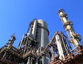
ASE Technology Holding Co. Ltd. (NYSE:ASX) has unveiled plans to commercialise an industry-first automated panel-level semiconductor packaging production line, marking another step in the evolution of advanced chip manufacturing. The new platform is expected to support next-generation artificial intelligence, high-performance computing (HPC) and edge computing applications by improving manufacturing efficiency and packaging density. As demand for increasingly powerful semiconductor solutions continues expanding, advanced packaging technologies are becoming a key competitive differentiator across the global chip industry. The latest development also reinforces growing interest across AI Stocks as semiconductor infrastructure continues supporting the rapid adoption of artificial intelligence technologies.
Advanced packaging becomes increasingly important
Semiconductor packaging has become a major area of innovation as chip complexity continues increasing.
Modern processors increasingly rely on advanced packaging techniques to improve performance, reduce power consumption and integrate multiple processing components into a single package.
These technologies support applications including:
- Artificial intelligence
- High-performance computing
- Cloud infrastructure
- Edge computing
- Data centres
Advanced packaging is therefore becoming as important as semiconductor fabrication itself.
Panel-level packaging expands manufacturing efficiency
ASE's new production platform replaces traditional circular semiconductor wafers with larger rectangular manufacturing panels.
This approach increases available manufacturing surface area while improving production efficiency.
Potential advantages include:
- Greater material utilisation
- Higher production throughput
- Improved manufacturing scalability
- Lower production costs
- Increased packaging density
These improvements are expected to support increasingly sophisticated semiconductor designs.
Artificial intelligence continues driving semiconductor demand
Artificial intelligence remains one of the strongest structural growth drivers for the semiconductor industry.
Growing deployment of AI systems continues increasing demand for:
- AI accelerators
- Graphics processors
- Advanced memory
- Chiplet architectures
- High-speed interconnect technologies
Packaging technologies capable of supporting these increasingly complex systems continue attracting significant industry investment.
Chiplet architectures reshape semiconductor design
Modern semiconductor development increasingly relies on chiplet-based designs rather than traditional monolithic processors.
Chiplets allow manufacturers to combine multiple specialised processing components within a single package.
This approach offers several advantages:
Improved scalability
Chiplets allow more flexible processor configurations.
Better manufacturing efficiency
Smaller semiconductor components may improve production yields.
Enhanced performance
Advanced packaging supports faster communication between processing units.
Greater design flexibility
Manufacturers can integrate different technologies within one package.
These trends continue driving demand for advanced packaging platforms.
AI infrastructure investment continues accelerating
Technology companies continue investing heavily in artificial intelligence infrastructure.
Growing investment spans multiple areas including:
- Semiconductor manufacturing
- Cloud computing
- Data centres
- Advanced networking
- High-performance processors
Advanced semiconductor packaging forms an essential part of this broader technology ecosystem.
Compatibility supports broader adoption
ASE's new panel-level packaging platform is expected to remain compatible with its existing packaging technologies.
Maintaining compatibility allows customers to continue using established semiconductor design approaches while benefiting from improved manufacturing capabilities.
Technology continuity often supports smoother commercial adoption across existing semiconductor supply chains.
Semiconductor manufacturing continues evolving
The semiconductor industry continues experiencing rapid technological advancement.
Manufacturers increasingly focus on:
- Advanced packaging
- Manufacturing automation
- Material efficiency
- Process innovation
- Production scalability
These developments continue supporting next-generation computing applications.
Global demand remains supported
Artificial intelligence, cloud computing and digital transformation continue supporting long-term semiconductor demand.
Growing computational requirements across enterprise and consumer technologies continue driving innovation throughout semiconductor manufacturing.
Advanced packaging technologies are expected to play an increasingly important role as processor complexity continues expanding.
Looking ahead
Future attention is likely to remain focused on:
- Production line development
- Manufacturing readiness
- Commercial deployment
- Customer adoption
- Semiconductor packaging innovation
These milestones will provide greater insight into the commercial rollout of ASE's next-generation manufacturing platform.
ASE Technology continues strengthening its position within the semiconductor industry through development of an automated panel-level packaging platform designed for artificial intelligence and high-performance computing applications. As advanced packaging becomes increasingly important across next-generation semiconductor manufacturing, innovations supporting greater efficiency, scalability and performance are expected to remain central to future industry growth.
