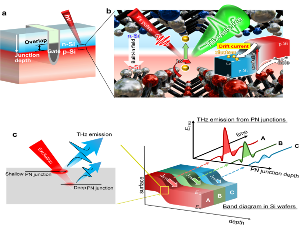
GA, UNITED STATES, June 21, 2025 /EINPresswire.com/ -- An international research group successfully measured, with a nanometer resolution, the depth of PN junctions varied in a Si wafer in a non-destructive and non-contact manner by observing the THz waves generated by irradiating a Si wafer with a femtosecond laser. The technique will open new avenues for developing advanced semiconductor devices, such as 3D LSI, and provide a comprehensive measurement solution that enables non-contact testing in semiconductor manufacturing.
Si LSI manufacturing technology is essential as the foundation of modern society. However, there was no wafer-scale technology for rapid, non-destructive, and non-contact evaluation of the internal electric field distribution, carrier transport characteristics, defects, and high-speed response of devices, which are being miniaturized and made three-dimensional to achieve high-density integration of electronic devices.
In a new paper published in Light: Science & Applications, an international team of scientists from Okayama University, Rice University, the Samsung Japan Research Institute Group, and the Samsung Electronics Group, led by Professor Masayoshi Tonouchi from Research Institute for Interdisciplinary Science, Okayama University, Japan, has developed a new method to estimate the PN junction depth formed shallowly in the Si wafer with a nanometer scale resolution in a non-destructive and non-contact manner for the first time.
The PN junction formed inside the wafer is illuminated with a femtosecond laser (an ultrashort pulse laser), and the terahertz electromagnetic waves (THz waves) are successfully measured due to the photocarrier generation at the PN junctions. As shown in Figure 1, the excited photo-carriers are accelerated at the depletion region in the direction of the n-type Si layer for electrons and in the direction of the p-type Si layer for holes. The instantaneous current generated at this time excites THz waves, which propagate to the surface and are radiated into space.
Prof. Tonouchi emphasized, “The THz waves are essentially generated through the complicated ultrafast photocarrier behavior, but by employing the simple model of the behavior, one can understand the movement of the carriers intuitively and evaluate the depth of the PN junction. Here, we introduce the depth estimation procedure with the simple mode for the THz eave generation from PN junctions for the first time.”
Young scientist Dr. Murakami explained, “It was tricky to use shorter laser wavelengths to excite the shallow PN junctions of Si because the penetration depth of the typical femtosecond laser with a wavelength odd use the f around 800 nm, is much longer than 10 micrometers for Si, and so, we cannot expect that the method is available to characterizing the shallow PN junctions in Si wafers at first. We found that a half wavelength is suitable in the present case, and by tuning the wavelength, one can evaluate shallower junctions more precisely.”
“The complexity of semiconductor devices is accelerating as they aim for higher levels of integration, and the demands and issues for semiconductor wafer and device evaluation technology are increasing. This technology, which enables rapid, non-destructive, and non-contact access to the interior of wafers, which was difficult with existing analysis technology, brings about an important innovation to solve this problem. The results of this research are expected to provide not only the evaluation of wafer structures for devices, but also to provide a comprehensive measurement solution that enables non-contact testing in the semiconductor manufacturing process, which contributes to improving device reliability and reducing the resources consumed in the manufacturing process,” the scientists forecast.
References
DOI
10.1038/s41377-025-01911-0
Original Source URL
https://doi.org/10.1038/s41377-025-01911-0
Funding information
JSPS KAKENHI Grant No. JP 23H00184 partly supported this work.
Lucy Wang
BioDesign Research
email us here
Legal Disclaimer:
EIN Presswire provides this news content "as is" without warranty of any kind. We do not accept any responsibility or liability for the accuracy, content, images, videos, licenses, completeness, legality, or reliability of the information contained in this article. If you have any complaints or copyright issues related to this article, kindly contact the author above.
![]()


