


Highlights
- Major asset management firms have revised their positions in Photronics Inc.
- Institutional activity includes adjustments by Geode Capital Management and Boston Partners.
- Photronics continues to operate across multiple global regions in the semiconductor industry.
Manufacturing Support for the Semiconductor Ecosystem
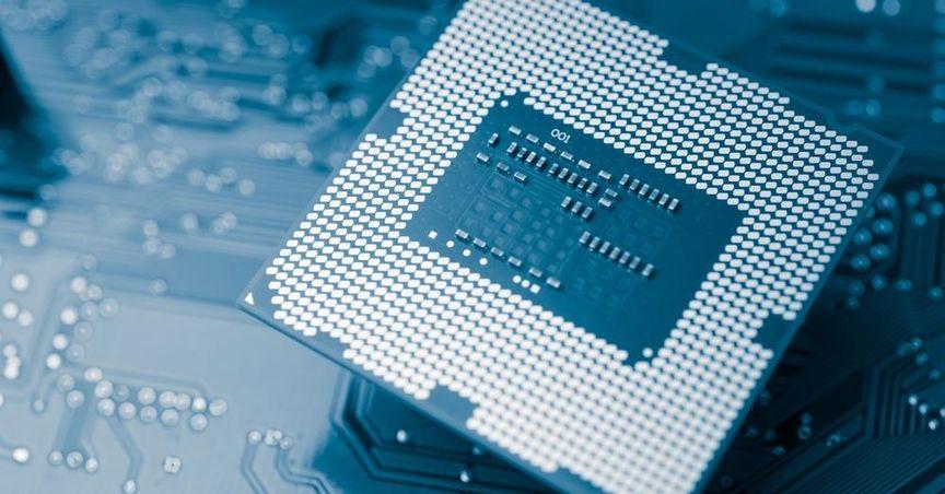
Photronics Inc. (NASDAQ:PLAB) operates in the semiconductor industry, providing essential components required in the manufacturing of integrated circuits and flat panel displays. The company specializes in photomasks, which are critical to the process of producing semiconductors used in consumer electronics, communications systems, and industrial devices. Photronics maintains manufacturing and distribution capabilities across the United States, Asia, and Europe, contributing to its presence in the global supply chain.
With a core focus on advanced photolithography support, Photronics plays a technical role in enabling the fabrication of microelectronic products. Its production model serves several key industries that rely on high-precision patterning and substrate technologies.
Institutional Activity Across Key Asset Firms
Recent reporting has shown notable institutional adjustments involving Photronics. Geode Capital Management made changes to its position, accompanied by portfolio activity from other financial groups including Boston Partners and Norges Bank. These firms adjusted their allocations in a period that saw increased attention toward semiconductor manufacturing and component suppliers.
The continued engagement from these institutions adds to a broader trend of reallocations in companies supporting semiconductor infrastructure. These firms have focused their exposure on businesses tied to fabrication materials and high-demand manufacturing equipment.
Business Operations and Regional Engagement
Photronics operates in several critical semiconductor hubs, including Taiwan, Korea, China, and the United States. These regions represent key areas for semiconductor production and research. The company’s strategic presence in these markets supports timely delivery and operational responsiveness to client requirements.
Through a network of cleanroom facilities and production centers, Photronics supplies a range of products supporting logic, memory, and display technology development. Its business segments also include collaborations with local and international customers in high-tech manufacturing sectors.
Performance Within the Semiconductor Segment
Photronics has maintained activity in segments that require technical precision and consistency in manufacturing. This includes engagement with companies producing display panels and electronic components. The structure of its services supports various end markets that rely on quality control and image clarity, both essential in semiconductor and display production.
The company’s operations remain integral to maintaining production schedules in the fabrication of advanced electronics. These functions contribute to continuity in global supply chains and are part of a larger framework supporting the evolution of chip and display technologies.
Broader Participation by Financial Firms
Adjustments by multiple asset management groups reflect a continued focus on companies engaged in semiconductor materials and equipment. These changes are often part of broader rebalancing activities in sectors aligned with technological manufacturing. Photronics, with its global facilities and specialized offerings, remains within the scope of firms managing industrial and technology-oriented portfolios.
The company’s positioning within the photomask segment of the semiconductor space has maintained relevance among financial groups focusing on precision-based manufacturing and international operations.